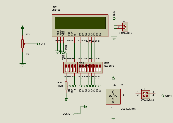
The HD44780 is a character LCD controller developed by HITACHI during the 1980s. So fa it still a popular stuff for electronics hobbyists, especially the Arduino user. The micro-processor should interface with this LCD using its 8-bit data bus mode. But using the 4-bit data bus mode is common for most electronics designers.
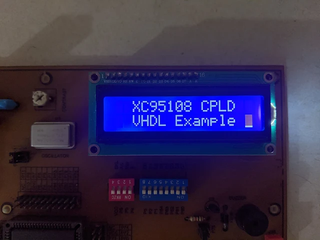
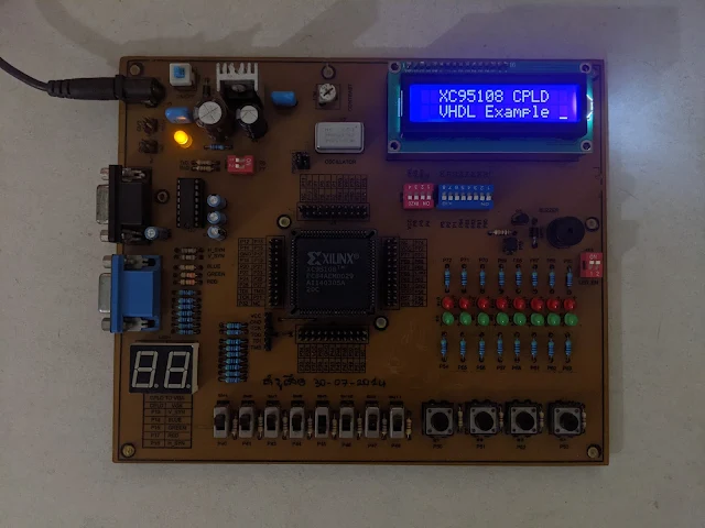
Hardware Test on the XC95108 Prototype Board |
A digital circuit also able to control this LCD module using a state machine model. If you are a beginner in digital electronics design you can see this post. In this VHLD example, I use an XC95108 CPLD to interface with this LCD controller using the 8-bit data transfer mode. The LCD is a 16x2 character LCD. It will show text on both lines of the LCD. The text should be "XC95108 CPLD" on the first line, and "VHDL Example" on the second line.
---------------------------------------------------------------------------------- -- Company: -- Engineer: -- -- Create Date: 13:36:50 01/28/2024 -- Design Name: -- Module Name: lcd_control_1 - Behavioral -- Project Name: -- Target Devices: -- Tool versions: -- Description: -- -- Dependencies: -- -- Revision: -- Revision 0.01 - File Created -- Additional Comments: -- ---------------------------------------------------------------------------------- library IEEE; use IEEE.STD_LOGIC_1164.ALL; -- Uncomment the following library declaration if using -- arithmetic functions with Signed or Unsigned values --use IEEE.NUMERIC_STD.ALL; -- Uncomment the following library declaration if instantiating -- any Xilinx primitives in this code. --library UNISIM; --use UNISIM.VComponents.all; entity lcd_control_1 is Port ( RST : in STD_LOGIC; CLK : in STD_LOGIC; RS : out STD_LOGIC; RW : out STD_LOGIC; EN : out STD_LOGIC; DB : out STD_LOGIC_VECTOR(7 DOWNTO 0)); end lcd_control_1; architecture Behavioral of lcd_control_1 is SIGNAL E: STD_LOGIC:='0'; begin RW<='0'; -- CLOCK AND ENABLE SIGNAL PROCESS PROCESS(CLK,RST) VARIABLE COUNTER: INTEGER RANGE 0 TO 25175; BEGIN IF RST='0' THEN COUNTER:=0; EN<='0'; ELSIF CLK'EVENT AND CLK='1' THEN COUNTER:=COUNTER+1; IF(COUNTER=25175) THEN E<=NOT E; END IF; EN<=E; END IF; END PROCESS; -- LCD COMMAND AND DATA PROCESS PROCESS(E) VARIABLE COUNTER: INTEGER RANGE 0 TO 35; BEGIN IF RST='0' THEN COUNTER:=0; DB<=x"00"; RS<='0'; ELSIF E'EVENT AND E='1' THEN COUNTER:=COUNTER+1; CASE COUNTER IS -- START UP DELAY WHEN 0 => WHEN 1 => WHEN 2 => -- LCD COMMAND WHEN 3 => RS<='0'; DB<=x"38"; WHEN 4 => RS<='0'; DB<=x"0F"; WHEN 5 => RS<='0'; DB<=x"01"; WHEN 6 => RS<='0'; DB<=x"06"; WHEN 7 => RS<='0'; DB<=x"82"; -- LCD DATA "XC95108 " WHEN 8 => RS<='1'; DB<=x"58"; WHEN 9 => RS<='1'; DB<=x"43"; WHEN 10 => RS<='1'; DB<=x"39"; WHEN 11 => RS<='1'; DB<=x"35"; WHEN 12 => RS<='1'; DB<=x"31"; WHEN 13 => RS<='1'; DB<=x"30"; WHEN 14 => RS<='1'; DB<=x"38"; WHEN 15 => RS<='1'; DB<=x"20"; -- LCD DATA "CPLD" WHEN 16 => RS<='1'; DB<=x"43"; WHEN 17 => RS<='1'; DB<=x"50"; WHEN 18 => RS<='1'; DB<=x"4C"; WHEN 19 => RS<='1'; DB<=x"44"; -- LCD COMMAND SECOND LINE POSITION 2 WHEN 20 => RS<='0'; DB<=x"C2"; -- LCD DATA "VHDL " WHEN 21 => RS<='1'; DB<=x"56"; WHEN 22 => RS<='1'; DB<=x"48"; WHEN 23 => RS<='1'; DB<=x"44"; WHEN 24 => RS<='1'; DB<=x"4C"; WHEN 25 => RS<='1'; DB<=x"20"; -- LCD DATA "Example " WHEN 26 => RS<='1'; DB<=x"45"; WHEN 27 => RS<='1'; DB<=x"78"; WHEN 28 => RS<='1'; DB<=x"61"; WHEN 29 => RS<='1'; DB<=x"6D"; WHEN 30 => RS<='1'; DB<=x"70"; WHEN 31 => RS<='1'; DB<=x"6C"; WHEN 32 => RS<='1'; DB<=x"65"; WHEN 33 => RS<='1'; DB<=x"20"; WHEN 34 => RS<='0'; DB<=x"00"; WHEN OTHERS => COUNTER:=34; END CASE; END IF; END PROCESS; end Behavioral;
The on-board oscillator is 25.175MHz. So I need to add a VHDL clock divider circuit to get a 1kHz signal.
The on-board oscillator is 25.175MHz |
Data or command are latched into the LCD controller from logic high low. So at the high logic level the circuit starts send data or command to the LCD. Then they will be latched into the LCD at the up coming logic low.
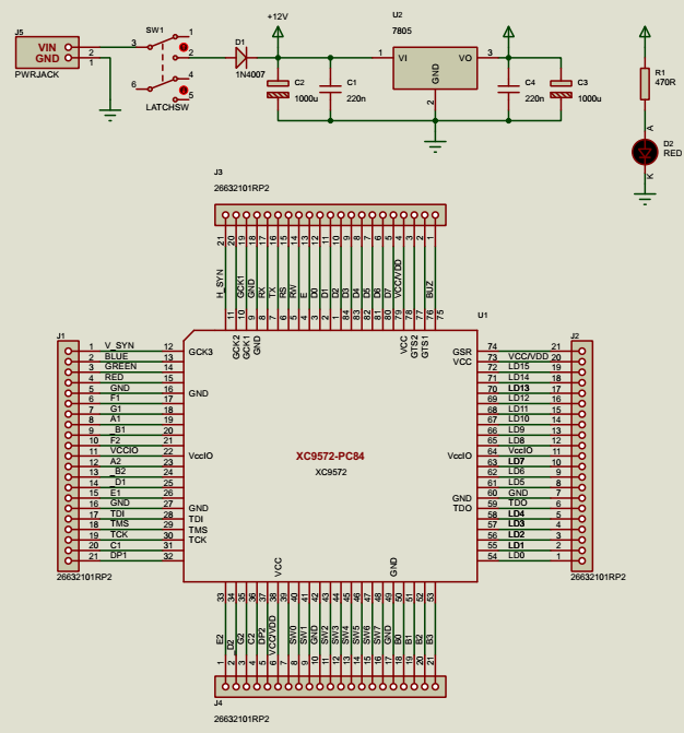
Main CPLD Prototype Board Block |
Character LCD and Oscillator |
#PACE: Start of Constraints generated by PACE
#PACE: Start of PACE I/O Pin Assignments
NET "CLK" LOC = "P9" ;
NET "DB<0>" LOC = "P2" ;
NET "DB<1>" LOC = "P1" ;
NET "DB<2>" LOC = "P84" ;
NET "DB<3>" LOC = "P83" ;
NET "DB<4>" LOC = "P82" ;
NET "DB<5>" LOC = "P81" ;
NET "DB<6>" LOC = "P80" ;
NET "DB<7>" LOC = "P79" ;
NET "EN" LOC = "P3" ;
NET "RS" LOC = "P5" ;
NET "RST" LOC = "P40" ;
NET "RW" LOC = "P4" ;
#PACE: Start of PACE Area Constraints
#PACE: Start of PACE Prohibit Constraints
#PACE: End of Constraints generated by PACE
This digital circuit design uses 35 macro cells and 51 Function Block.
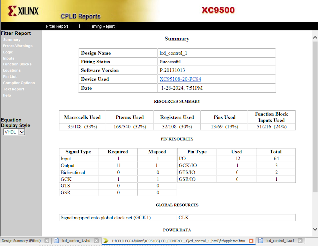
XC95108 CPLD Reports |
Using a Xilinx Parallel Cable III or IV is suitable for device programming in the Xilinx ISE Design Suite 14.7.
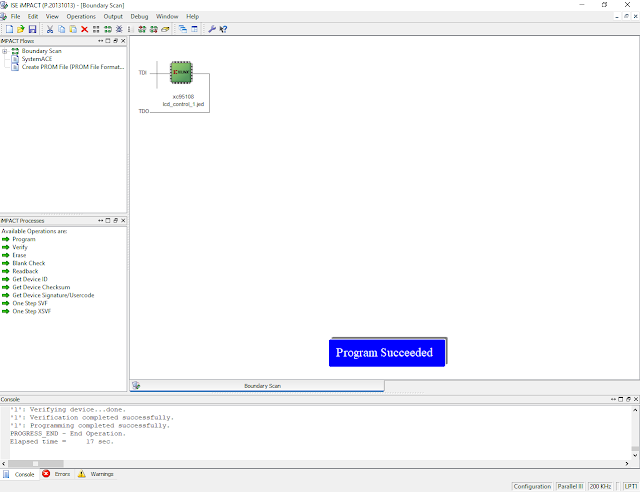
Device Programming Using a Xilinx Parallel Cable IV JTAG |
Click here to download its source file.
No comments:
Post a Comment