Sunday, December 17, 2023

XC9536 CPLD HD44780 8-Bit LCD Interfacing Example Using VHDL

Character LCD interfacing is very popular among electronics hobbyists. Using a minimum 8-bit microcontroller with Assembly language programming is very common. This simple 8-bit HD44780 character LCD can be tested manually by applying digital logic inputs by switches without using any controller.


Some electronics practitioners use a digital circuit created by some digital logic chips to control this character LCD. Similarly a Programmable Logic Device (PLD) can replace that complex digital electronics circuit. We can use schematic design or even an easier VHDL or Verilog coding to design an LCD interface circuit that will run on any CPLD or FPGA.
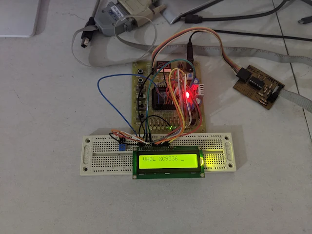
XC9536 CPLD HD44780 8-Bit LCD Interfacing Example Using VHDL
VHDL Code Testing on an experiment board

In this VHDL example, I use an old simple Complex Programmable Logic Device (CPLD) to create a digital electronics circuit inside to interface with a HD44780 based character LCD module.  

Using a Finite State Machine (FSM) model is very common this task. However I didn't follow all of this FSM model. I use a counter to activate each steps of data transfer between CPLD and LCD module.

An on-board 60Hz square wave oscillator is needed to active the circuit. LCD data and command are sequentially send to the LCD. It activated only at the high logic level of Enable (EN) output pin.

I use a low cost Chinese JHD162A LCD module. It costs around 2USD at local store.

XC9536 CPLD HD44780 8-Bit LCD Interfacing Example Using VHDL
JHD162A LCD Module Interfacing Pins

The following VHDL codes will show a "VHDL XC9536" message on a character LCD. Then it will stop transferring data.

  1. ----------------------------------------------------------------------------------
  2. -- Company:
  3. -- Engineer:
  4. --
  5. -- Create Date: 16:57:52 12/16/2023
  6. -- Design Name:
  7. -- Module Name: lcd_8 - Behavioral
  8. -- Project Name:
  9. -- Target Devices:
  10. -- Tool versions:
  11. -- Description:
  12. --
  13. -- Dependencies:
  14. --
  15. -- Revision:
  16. -- Revision 0.01 - File Created
  17. -- Additional Comments:
  18. --
  19. ----------------------------------------------------------------------------------
  20. library IEEE;
  21. use IEEE.STD_LOGIC_1164.ALL;
  22.  
  23. -- Uncomment the following library declaration if using
  24. -- arithmetic functions with Signed or Unsigned values
  25. --use IEEE.NUMERIC_STD.ALL;
  26.  
  27. -- Uncomment the following library declaration if instantiating
  28. -- any Xilinx primitives in this code.
  29. --library UNISIM;
  30. --use UNISIM.VComponents.all;
  31.  
  32. entity lcd_8 is
  33. Port ( CLK : in STD_LOGIC;
  34. RST : in STD_LOGIC;
  35. RS : out STD_LOGIC;
  36. EN : out STD_LOGIC;
  37. DB : out STD_LOGIC_VECTOR (7 downto 0));
  38. end lcd_8;
  39.  
  40. architecture Behavioral of lcd_8 is
  41. signal E : STD_LOGIC:='0';
  42. begin
  43. clock: process(CLK,RST)
  44. variable ticks: INTEGER RANGE 0 TO 32:=0;
  45. begin
  46. if(RST='0') then ticks:=0; E<='0';
  47. elsif(CLK'EVENT AND CLK='1') then
  48. if(ticks<32) then
  49. ticks:=ticks+1;
  50. E<=E XOR '1';
  51. EN<=E;
  52. end if;
  53. end if;
  54. end process clock;
  55.  
  56. process(E)
  57. variable temp : INTEGER RANGE 0 TO 16;
  58. begin
  59. if(RST='0') then temp:=0; DB<=x"00";
  60. elsif(E'EVENT AND E='1') then
  61. temp:=temp+1;
  62. CASE temp IS
  63. WHEN 0 => RS<='0'; DB<=x"38"; -- 5x7 Two Lines
  64. WHEN 1 => RS<='0'; DB<=x"0F"; -- LCD On Cursor Blink
  65. WHEN 2 => RS<='0'; DB<=x"01"; -- Clear Screen
  66. WHEN 3 => RS<='0'; DB<=x"06"; -- LCD Shift Cursor Right
  67. ----------------------------------
  68. WHEN 4 => RS<='1'; DB<=x"56"; -- V
  69. WHEN 5 => RS<='1'; DB<=x"48"; -- H
  70. WHEN 6 => RS<='1'; DB<=x"44"; -- D
  71. WHEN 7 => RS<='1'; DB<=x"4C"; -- L
  72. WHEN 8 => RS<='1'; DB<=x"20"; -- SPACE
  73. WHEN 9 => RS<='1'; DB<=x"58"; -- X
  74. WHEN 10 => RS<='1'; DB<=x"43"; -- C
  75. WHEN 11 => RS<='1'; DB<=x"39"; -- 9
  76. WHEN 12 => RS<='1'; DB<=x"35"; -- 5
  77. WHEN 13 => RS<='1'; DB<=x"33"; -- 3
  78. WHEN 14 => RS<='1'; DB<=x"36"; -- 6
  79. WHEN 15 => RS<='1'; DB<=x"20"; -- SPACE
  80. WHEN 16 => RS<='1'; DB<=x"20"; -- SPACE
  81. WHEN OTHERS => NULL;
  82. END CASE;
  83. end if;
  84. end process;
  85. end Behavioral;
  86.  
  87.  

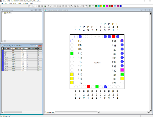
Don't forget to assign its I/O pins. The LCD 8-bit data bus shares with on-board LEDs.
XC9536 CPLD HD44780 8-Bit LCD Interfacing Example Using VHDL
Xilinx PACE Tool - I/O Pin Assignments

We will need to run the Implement Design again to wire its I/O pins. We will see its CPLD Reports.

XC9536 CPLD HD44780 8-Bit LCD Interfacing Example Using VHDL
CPLD Reports

If you have a Desktop computer with a legacy parallel port we can use a Xilinx Parallel Cable III JTAG to program this CPLD. However a modern USB JTAG is currently widely used with an affordable price. A USB JTAG cable is very stable to use than a legacy one's.


Click here to download its VHDL, UCF, and JED files.
Friday, December 15, 2023

XC9536 SPI Two-Digit Multiplexing Display Driver

In this VHDL example, I design a Serial Peripheral Interface (SPI) receiver circuit that can drive a two-digit multiplexing display. The SPI receiver module is similar to a SN74HC164 serial-in-parallel-out shift registers. This module contains two shift registers inside. These two registers connects individually connect to two output port that drive to a two-digit multiplexing display. 

XC9536 SPI Two-Digit Multiplexing Display Driver
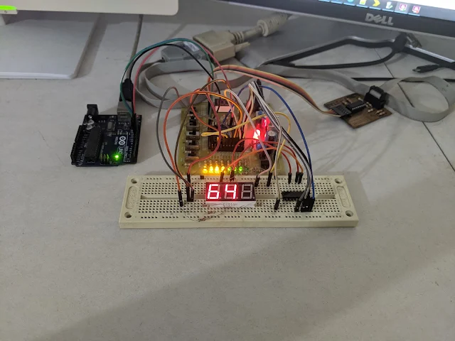
I an Arduino Uno to send a serial data package over the SPI to the XC9536 CPLD on board. 


SPI module does not need internal clock source. But the multiplexing display module needs a clock source to drive its output display at a rate of 16 milliseconds. I use an NE555 square wave oscillator to create a timing signal with a frequency of 60Hz for multiplexing display driving.

This design contains two process one's for SPI receiver module, and another one's for multiplexing display driving. These two processes are concurrent so the multiplexing display process does not need to wait or get interrupted by the SPI receiving process.

  1. ----------------------------------------------------------------------------------
  2. -- Company:
  3. -- Engineer:
  4. --
  5. -- Create Date: 08:34:17 12/15/2023
  6. -- Design Name:
  7. -- Module Name: spi_display_2 - Behavioral
  8. -- Project Name:
  9. -- Target Devices:
  10. -- Tool versions:
  11. -- Description:
  12. --
  13. -- Dependencies:
  14. --
  15. -- Revision:
  16. -- Revision 0.01 - File Created
  17. -- Additional Comments:
  18. --
  19. ----------------------------------------------------------------------------------
  20. library IEEE;
  21. use IEEE.STD_LOGIC_1164.ALL;
  22.  
  23. -- Uncomment the following library declaration if using
  24. -- arithmetic functions with Signed or Unsigned values
  25. --use IEEE.NUMERIC_STD.ALL;
  26.  
  27. -- Uncomment the following library declaration if instantiating
  28. -- any Xilinx primitives in this code.
  29. --library UNISIM;
  30. --use UNISIM.VComponents.all;
  31.  
  32. entity spi_display_2 is
  33. Port ( OSC : in STD_LOGIC;
  34. RST : in STD_LOGIC;
  35. TEST: in STD_LOGIC;
  36. SCLK : in STD_LOGIC;
  37. SDAT : in STD_LOGIC;
  38. COM : out STD_LOGIC_VECTOR (1 downto 0);
  39. LED : out STD_LOGIC_VECTOR (7 downto 0));
  40. end spi_display_2;
  41.  
  42. architecture Behavioral of spi_display_2 is
  43. signal reg_0,reg_1 : STD_LOGIC_VECTOR(7 DOWNTO 0):=x"00";
  44.  
  45. begin
  46. -- SPI Receiver Block
  47. spi_receive: process(SCLK,RST)
  48. begin
  49. if(RST='0') then
  50. reg_0<=x"00"; reg_1<=x"00";
  51. elsif(SCLK'EVENT AND SCLK='1') then
  52. -- Serial Data Receive
  53. reg_0(0)<=SDAT;
  54. reg_0(1)<=reg_0(0);
  55. reg_0(2)<=reg_0(1);
  56. reg_0(3)<=reg_0(2);
  57. reg_0(4)<=reg_0(3);
  58. reg_0(5)<=reg_0(4);
  59. reg_0(6)<=reg_0(5);
  60. reg_0(7)<=reg_0(6);
  61.  
  62. reg_1(0)<=reg_0(7);
  63. reg_1(1)<=reg_1(0);
  64. reg_1(2)<=reg_1(1);
  65. reg_1(3)<=reg_1(2);
  66. reg_1(4)<=reg_1(3);
  67. reg_1(5)<=reg_1(4);
  68. reg_1(6)<=reg_1(5);
  69. reg_1(7)<=reg_1(6);
  70.  
  71. end if;
  72.  
  73. end process spi_receive;
  74.  
  75. -- Multiplexing Display Block
  76. display_multiplex: process(OSC,RST)
  77. variable ticks : INTEGER RANGE 0 TO 1:=0;
  78. begin
  79. if(RST='0') then ticks:=0; COM<="00"; LED<=x"00";
  80. elsif(OSC'EVENT AND OSC='1') then
  81. ticks:=ticks+1;
  82. if(test='1') then
  83. CASE ticks IS
  84. WHEN 0 => LED<=reg_0; COM<="01";
  85. WHEN 1 => LED<=reg_1; COM<="10";
  86. WHEN OTHERS => NULL;
  87. END CASE;
  88. else
  89. CASE ticks IS
  90. WHEN 0 => LED<=x"3F"; COM<="01";
  91. WHEN 1 => LED<=x"06"; COM<="10";
  92. WHEN OTHERS => NULL;
  93. END CASE;
  94. end if;
  95. end if;
  96. end process display_multiplex;
  97. end Behavioral;
  98.  
  99.  

As we can see the display has three digits but I can use only two digits because the XC9536 CPLD has limited resource. I can not add one more shift registers signal.

I assign all of its I/O pins as follow.

XC9536 SPI Two-Digit Multiplexing Display Driver
Xilinx PACE

Its user constraints file is automatically generated after the Xilinx PACE is saved.

#PACE: Start of Constraints generated by PACE
#PACE: Start of PACE I/O Pin Assignments
NET "COM<0>"  LOC = "P42"  ; 
NET "COM<1>"  LOC = "P43"  ; 
NET "LED<0>"  LOC = "P33"  ; 
NET "LED<1>"  LOC = "P34"  ; 
NET "LED<2>"  LOC = "P35"  ; 
NET "LED<3>"  LOC = "P36"  ; 
NET "LED<4>"  LOC = "P37"  ; 
NET "LED<5>"  LOC = "P38"  ; 
NET "LED<6>"  LOC = "P39"  ; 
NET "LED<7>"  LOC = "P40"  ; 
NET "OSC"  LOC = "P5"  ; 
NET "RST"  LOC = "P25"  ; 
NET "SCLK"  LOC = "P18"  ;
NET "SDAT"  LOC = "P19"  ;
NET "TEST"  LOC = "P26"  ; 
#PACE: Start of PACE Area Constraints
#PACE: Start of PACE Prohibit Constraints
#PACE: End of Constraints generated by PACE


I still use a Xilinx Parallel Cable III to program this CPLD.

XC9536 SPI Two-Digit Multiplexing Display Driver
Xilinx iMPACT Tools

We don't need to press the SPI serial data and serial clock manually. We just use an Arduino Uno board to send SPI data to this board. The Arduino uses three pins, MOSI, SCK, and reset to connect to the CPLD. 

The Arduino program below sends a counting variable ranging from 0 to 99 to the CPLD.

  1. #include<SPI.h>
  2.  
  3. void setup() {
  4. SPI.begin();
  5. pinMode(10,OUTPUT);
  6. digitalWrite(10,LOW);
  7. delay(1);
  8. digitalWrite(10,HIGH);
  9. SPI.transfer(0x3F);
  10. SPI.transfer(0x3F);
  11. delay(2500);
  12. }
  13.  
  14. int count=0;
  15. const char _7_SEG[10]={0x3F,0x06,0x5B,0x4F,0x66,0x6D,0x7D,0x07,0x7F,0x6F,};
  16. void loop() {
  17. SPI.transfer(_7_SEG[count%10]);
  18. SPI.transfer(_7_SEG[count/10]);
  19. delay(250);
  20. count++;
  21. if(count>99) count=0;
  22.  
  23. }

This program sends a random decimal number between 0 and 99 to the CPLD board.

  1. #include<SPI.h>
  2.  
  3. void setup() {
  4. SPI.begin();
  5. pinMode(10,OUTPUT);
  6. digitalWrite(10,LOW);
  7. delay(1);
  8. digitalWrite(10,HIGH);
  9. SPI.transfer(0x3F);
  10. SPI.transfer(0x3F);
  11. delay(2500);
  12. }
  13.  
  14. int myNumbers;
  15. const char _7_SEG[10]={0x3F,0x06,0x5B,0x4F,0x66,0x6D,0x7D,0x07,0x7F,0x6F,};
  16. void loop() {
  17. myNumbers=random(99);
  18. SPI.transfer(_7_SEG[myNumbers%10]);
  19. SPI.transfer(_7_SEG[myNumbers/10]);
  20. delay(500);
  21. }

Click here to download its source file.


Labels

ADC (10) Analog (14) Arduino (12) Atmega16 (19) Audio (2) AVR (20) Charger (1) Cortex-M0 (1) Counter (10) CPLD (25) Digital I/O (22) Display (34) EEPROM (2) Environment Sensor (1) esp8266 (2) Experiment Board (10) I2C (4) Interrupt (7) LCD (1) LDmicro (29) measurement and instrumentation (7) Microchip Studio (3) MikroC (1) One-Shot (3) OpAmp (1) PCB (31) PIC16 Microcontrollers (16) PIC16F877A (2) PIC16F887 MikroC (22) PLC (35) PWM (11) Regulator (1) RTC (2) Sensor (8) Shift Registers (5) SPI (5) Timer (34) UART (2) ultra-sonic sensor (1) USB (1) VHDL (21) xc8 (1) XC95108 (9) XC9536 (15) XC9572 (1) Xilinx (23) Xilinx ISE (22)