Overview
The development board for any microcontroller are widely available especially in the online market place. They come with various peripheral device and programming examples.
The Atmel (Now Microchip) AVR microcontroller is one of the most popular microcontroller in-use today. The development boards for this device are available. They are ready to use with a select-able scale and price.
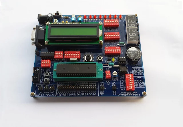 |
| The final test of the board with error free |
For an electronic hobbyist or student, a development could be built using a single board PCB with a minimum on-board peripheral devices. Using a development board, the prototyping and testing are safer and time saving.
With a PCB fabrication service support, I decided to design a development board for the Atmel AVR ATMega16 microcontroller for my own microcontroller experiments.
Features
The design comes with many features that fully work with the ATMega16 chip:
- Digital inputs and outputs
- analog input devices
- Display
- RS-232
- SPI peripheral device
- TWI peripheral devices etc.
It mentions only the ATMega16 chip. However, the board supports other AVR devices with the 40-pin DIP package. I have tested this board with some chips I posses:
- ATMega16
- ATMega32
- ATMega644
I think it works with the ATMega1284. But currently I don’t have this chip in my own laboratory.
The PCB Design
The completed design made with a free EDA software. It takes almost a week to finish the schematic and PCB design.
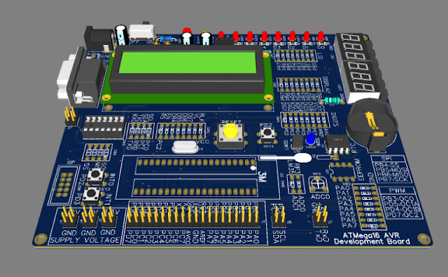 |
| The finished design of this development board |
The schematic design need up to two letter size sheet.
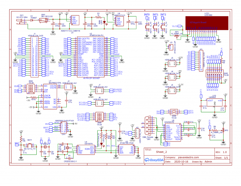 |
| Schematic Sheet2 |
 |
| Schematic Sheet1 |
Within the design most of the resistors and the capacitors are in the SMD package. The PCB size is a little bigger than 10 cm square. I didn’t plan about the target of the PCB.
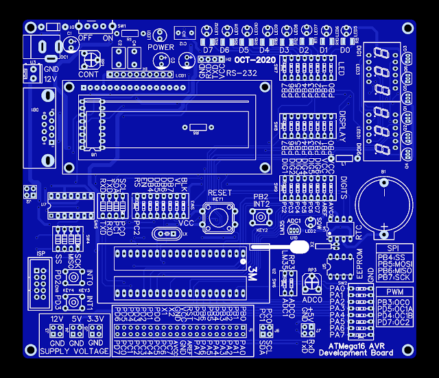 |
| Top Layer |
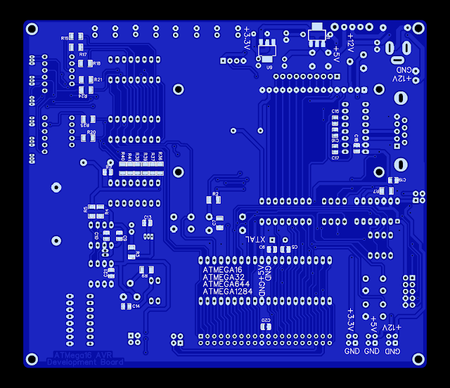 |
| Bottom Layer |
Within the design most of the resistors and the capacitors are in the SMD package. The PCB size is a little bigger than 10 cm square. I didn’t plan about the target of the PCB.
On Board Resource
Beside the DC power supply circuit, all other components have their own unique function connect to the microcontroller.
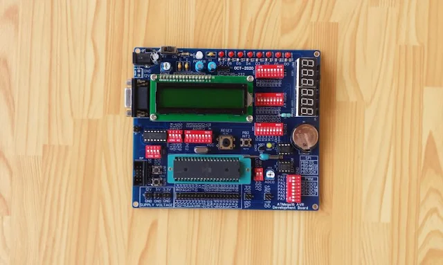 |
| This board is just ready after a few hours of the assembling/soldering. |
DC Regulated Power Supply
An AC to DC converter is need to power this board. All on-board component supplies from a +5V regulated IC – AMS1117-5.0. There is an optional +3.3V regulated IC – AMS1117-3.3 that could be useful for others low voltage devices.
 |
| The power supply circuit |
Microcontroller Clock And Reset Circuit
The on-board ATMega16 chip supplies at +5V DC. Clock and reset circuit are already wired with this chip on board.
 |
| Reset and Clock for the ATMega16 |
In System Programming
The in System Programming (ISP) is an appropriate flash memory upload tool for the Microchip AVR chip. Currently, most of the ISP programmers are very low cost as a result of the open-source tool.
 |
| ISP header for this ATMega16 development board – It follows the USBasp programming header. |
This header is a 10-pin IDC header/connector. It fits the USBasp programmer that connects externally.
RS-232
The RS-232 communicate between a host PC with the on-board microcontroller. This communication could be very classic now. The recent development replaces this interface with a USB-Serial converter chip. This new technology is very effective in cost and size.
 |
| The RS-232 circuit – The Tx/Rx of the host PC side will connect to the on-board microcontroller across a DIP switch. |
However I still have the HIN232/MAX232 RS232 level converter that still has a few left in my workshop.
Digital Input/Output
The basic digital input/output on this board made of two distinct ports. PORTB is for output that connects to a 8-bit LED.
 |
| A DIP switch enables or disables the output to LED |
 |
| PORTA connects to a DIP switch. When it’s on a low logic value is created. |
All digital input pins of the ATMega16 have their own weak pull-up resistor that will be turn on by software.
Multiplexed Display
A multiplexed display created by a numbers of seven-segments LED displays. Each digit of the multiplexed display shares the same segments. Each common of the display turns on and off the digit.
 |
| A six-digits multiplexed display. Two distinct DIP swith enables and disables the connection to the microcontroller. |
The display in-use here is a 0.36″ common cathode display. PORTB connects the segments across a DIP switch while PORTC controls the six-digits common of the seven-segments. The SW8 DIP switch has a two remaining pins, allowing the user to configure the voltage reference pins for the microcontroller’s ADC.
Analog to Digital Converter
The Analog to Digital Converter (ADC) module built inside the ATMega16 chip. PORTA is multiplexed with the ADC inputs – ADC0 to ADC7.
 |
| Two ADC inputs – The LM35DZ and a trim POT |
External Interrupts
The external interrupts of the ATMega16 creates by three distinct pins, name INT0, INT1 and INT2.
 |
| External interrupt mechanism |
A typical tactile switch creates an interrupt to the microcontroller. On this board it happens at the low logic level of the input.
Character LCD
A character LCD developed by Hitachi has been popular for a few decades. It still in-use now for education purpose.
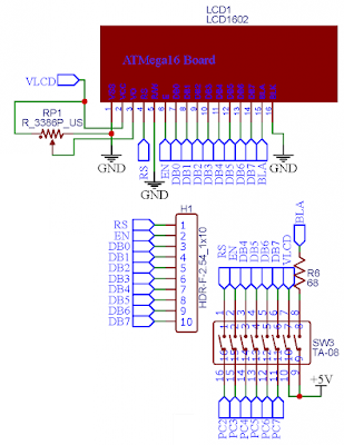 |
| The Hitachi HD44780 character LCD interfaces in 4-bit mode. |
Serial Peripheral Interface
The Serial Peripheral Interface (SPI) of the ATMega16 chip here connects to a 12-bit Digital to Analog Converter (DAC) across a DIP switch. The preset analog voltage reference of the DAC chip is to +5V.
 |
| The MCP4922 dual 12-bit DAC connects to the ATMega16 SPI |
Two-wire Serial Communication
The Two-wire serial communication (TWI) originally known as the Inter-integrated Circuit (I2C) requires only two electrical communication lines on a single bus to command and exchange the data. On this board I put two TWI chips – a DS1307 Real Time Clock (RTC) and an AT24C16 EEPROM.
 |
| The TWI communication interface to the ATMega16 |
A DIP switch SW5 allows the connection between the TWI block and the microcontroller. Optionally this gate is bridge between the RS-232 and the microcontroller.
Connectors And Headers
This board allow an external connection to the outside device via many pre-soldered connectors/headers. The main ATMega16 chip with its 40-pin wires to a 2×20 on-board male header. Other headers are,
- The DC power supplies outputs – +12V, +5V and +3.3V DC.
- The SPI output
- The TWI external connection
- The USART external connection etc
They are labeled on the development board.
Ordering A PCB
As it’s often mentioned, using a service from a PCB fab gives more advantage for a complex design circuit board. The PCB of this ATMega16 development board was ordered from PCBWay. The company provides the PCB fabrication service up to 14 layers. Getting the PCB delivered to my warehouse within a few days saves a lot of time and engineering cost.
 |
| A pack of PCB from PCBWay |
 | |||
| Unboxing the PCB #1 |
Soldering And Assembling
Ordering the PCB from a fabrication service gives some advantages to the students and hobbyists:
- It’s easy to solder as the soldering pads are plated with some soldering friendly materials – lead, lead free, immersion silver and up to the hard gold. These materials are very hard to get oxidized in the air if the PCB are kept for a long period.
- The components legend on both sides give the information to the solder man and the end user about the components placement and about the printed circuits.
- With the advantage of solder mask the PCB is very hard to become corrosive cause by some other chemical materials that it suffered. The solder mask color is select-able between various colors – green, blue, yellow etc. The green one’s is very convenient as it’s very easy for the user to observe the tracks.
I use a 40 W electrical soldering iron to solder all the components. The overall soldering/assembling processes take only a few hours.
 |
| A 40W gun type iron solder is suitable for this job |
 |
| Some components for soldering |
 |
| A finished assembling at top layer |
 |
| A finished assembling at the bottom layer |
I'm writing and testing sample program for Atmega16 for this board. They are releasing gradually.
ATMega644P Programming using AVR-LibC in Microchip Studio IDE (2025)
Recently I tested my ATMega644P chip that left from previous project. For more information please visit this page.
Microchip Studio is free of charge compiler provides by device manufacture. It comes with the GNU AVR-LibC that's widely used by many AVR programmers. However it only contains the standard C library functions. It has a little peripheral libraries. We need to write our own functions to interface with external hardware.
I recently test this chip by programming it using C. Some examples I tested using software simulator while others are tested using my AVR Prototype Board.
Basic I/O
 |
| Test Program |
- ATMega644P Input Output Programming Example
- ATMega644P External Interrupt Programming
- ATMega644P Pin Change Interrupt Example
LCD and Keypad Interfacing
- ATMega644P HD44780 Character LCD Interfacing
- ATMega644P LCD Display and Matrix Keypad Interface
- ATMega644P Graphical LCD Interfacing
Analog to Digital Converter (ADC)
 |
| Program Tested on my AVR Prototype Board |
Two Wire Interface (TWI) or Inter Integrated Circuit (I2C)
 |
| Date and Time Reading |
- ATMega644P TWI DS1307 and AT24C16 EEPROM Interfacing
- ATMega644P TWI PCF8574 I/O Expansion Interfacing
- ATMega644P TWI PCF8574AP Matrix Keypad LCD
- ATMega644P TWI LCD RTC and Keypad Example
- ATMega644P TWI MCP23017 GPIO Example
- ATMega644P TWI MCP23017 LCD Keypad
- ATMega644P TWI MCP23017 Character LCD


No comments:
Post a Comment