Wednesday, December 6, 2023

XC9536 Switch And LED Interfacing With Delay Using VHDL

Overview

In this VHDL example, I use an input push button to toggle an output LED. It also has a delay circuit that created by frequency divider. Signal source is generated by the on-board 60Hz NE555 square wave oscillator. 


XC9536 Switch And LED Interfacing With Delay Using VHDL
On-Board Testing


In VHDL It requires two I/O pin,

  1. LED - Output direction with STD_LOGIC type. It's assigned to pin 35 of XC9536 CPLD, connecting the on-board output LED.
  2. CLK - Input direction with STD_LOGIC type. It's assigned to pin 5 (GCK1) of XC9536 CPLD.
  3. BUTTON : Input direction STD_LOGIC type. It's assigned to pin 19, connecting to the on-board pulled up tactile switch. It's an active low signal.

A counter variable "count" holds a numeric value up to 60 counts. It's necessary for sequential circuit inside the process. A toggle signal with STD_LOGIC type is added for signal assignment to LED I/O pin. When a low to high clock pulse is activated at clock pin (CLK) it increases its content 1 time. Whenever it reaches 30 counts and the the input button "BUTTON" is pressed, it will be reset to 0. And the toggle signal will change its logic state. The LED logic state depends on the toggle signal.

VHDL Code

The VHDL code contains a dozen line of statements. Only one process evaluates the input and output. This process requires one sensitive parameter "CLK" in its list.

  1. ----------------------------------------------------------------------------------
  2. -- Company:
  3. -- Engineer:
  4. --
  5. -- Create Date: 21:49:59 12/05/2023
  6. -- Design Name:
  7. -- Module Name: Toggle_LED_CLK - Behavioral
  8. -- Project Name:
  9. -- Target Devices:
  10. -- Tool versions:
  11. -- Description:
  12. --
  13. -- Dependencies:
  14. --
  15. -- Revision:
  16. -- Revision 0.01 - File Created
  17. -- Additional Comments:
  18. --
  19. ----------------------------------------------------------------------------------
  20. library IEEE;
  21. use IEEE.STD_LOGIC_1164.ALL;
  22.  
  23. -- Uncomment the following library declaration if using
  24. -- arithmetic functions with Signed or Unsigned values
  25. --use IEEE.NUMERIC_STD.ALL;
  26.  
  27. -- Uncomment the following library declaration if instantiating
  28. -- any Xilinx primitives in this code.
  29. --library UNISIM;
  30. --use UNISIM.VComponents.all;
  31.  
  32. entity Toggle_LED_CLK is
  33. Port ( LED : out STD_LOGIC;
  34. CLK : in STD_LOGIC;
  35. BUTTON : in STD_LOGIC);
  36. end Toggle_LED_CLK;
  37.  
  38. architecture Behavioral of Toggle_LED_CLK is
  39.  
  40. signal toggle: STD_LOGIC;
  41.  
  42. begin
  43.  
  44. PROCESS (CLK)
  45. variable count : INTEGER RANGE 0 TO 59;
  46.  
  47. BEGIN
  48. if(CLK'EVENT AND CLK = '1') THEN
  49. count := count + 1;
  50. if(count>=30 AND BUTTON = '0') then
  51. toggle <= toggle XOR '1';
  52. count := 0;
  53. LED <= toggle;
  54. end if;
  55. end if;
  56. end process;
  57. end Behavioral;
  58.  
  59.  

Click here to download its source file. I want to know its RTL(Register Transfer Level) schematic.

XC9536 Switch And LED Interfacing With Delay Using VHDL
Register Transfer Level (RTL)


User Constraints

I don't use VHDL simulation here. This circuit will be constructed on an XC9536 CPLD using my test board. So I need to select the I/O pins before the program file is uploaded to CPLD.

Expand the User Constraints, and double click on the Floorplan IO to assign its I/O pins. And then save the document before we close it.

XC9536 Switch And LED Interfacing With Delay Using VHDL
I/O Pins Assignment


A user constraints file ".ucf" will be generated.

  1. #PACE: Start of Constraints generated by PACE
  2.  
  3. #PACE: Start of PACE I/O Pin Assignments
  4. NET "BUTTON" LOC = "P19" ;
  5. NET "CLK" LOC = "P5" ;
  6. NET "LED" LOC = "P35" ;
  7.  
  8. #PACE: Start of PACE Area Constraints
  9.  
  10. #PACE: Start of PACE Prohibit Constraints
  11.  
  12. #PACE: End of Constraints generated by PACE

After it's completed, we need to run the Implement Design to generated its program file ".jed". This file will be selected to program the target CPLD device.
XC9536 Switch And LED Interfacing With Delay Using VHDL
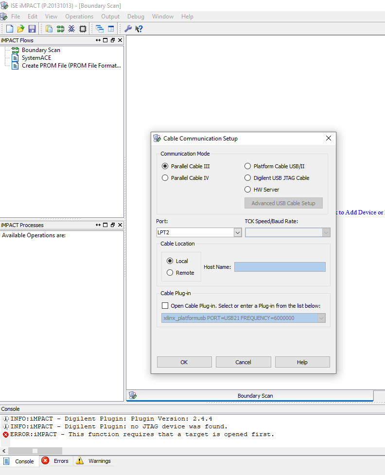
Cable Set Up - Select Parallel Cable III


I use the legacy parallel port interface connects to Parallel Cable III JTAG cable to program the target device. I use ISE Design Suites 14.7 running on Windows 10. My HP MT-6300 Desktop PC with parallel port still support this legacy I/O port. If you need a modern high speed USB JTAG, it works better than this old one's.
XC9536 Switch And LED Interfacing With Delay Using VHDL
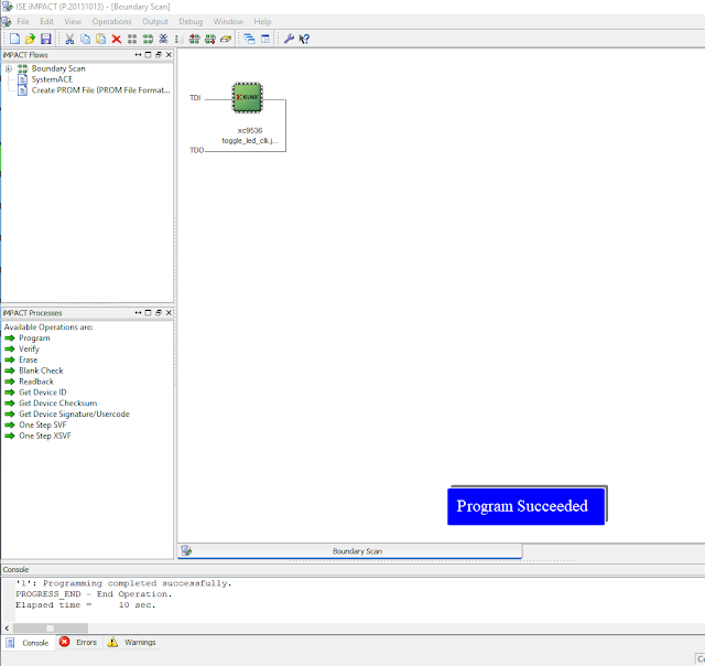
Programming 


Using this parallel port cable we need to be patient because of its low speed, and cable connection error.


No comments:

Post a Comment

Labels

ADC (10) Analog (14) Arduino (12) Atmega16 (19) Audio (2) AVR (20) Charger (1) Cortex-M0 (1) Counter (10) CPLD (25) Digital I/O (22) Display (34) EEPROM (2) Environment Sensor (1) esp8266 (2) Experiment Board (10) I2C (4) Interrupt (7) LCD (1) LDmicro (29) measurement and instrumentation (7) Microchip Studio (3) MikroC (1) One-Shot (3) OpAmp (1) PCB (31) PIC16 Microcontrollers (16) PIC16F877A (2) PIC16F887 MikroC (22) PLC (35) PWM (11) Regulator (1) RTC (2) Sensor (8) Shift Registers (5) SPI (5) Timer (34) UART (2) ultra-sonic sensor (1) USB (1) VHDL (21) xc8 (1) XC95108 (9) XC9536 (15) XC9572 (1) Xilinx (23) Xilinx ISE (22)