Introduction
A digital counter circuit can be made from scratch by using some digital ICs that contains a counter (eg, 74LS90), a 7-Segment decoder(eg, 74LS47), a 7-Segment display, a switch, and some passive components.
However we can use a microcontroller or even a programmable logic device to to such electronics stuff. Using a CPLD we can generate a digital circuit that able to replace some ASICs functionalities. An XC9536 CPLD can be used to design a small digital circuit with a little number of I/O.
 |
| Testing On Experiment Board |
I design a free running counter using VHDL code. It has a frequency divider, a counter, reset circuit, and a seven segment decoder inside. So we don't need to inter-connect between chips as the standard digital circuit does.
Design Tools
VHDL is simple to code. For XC9536 CPLD we can use ISE Design Suite. It's free for most of small CPLD and FPGA. Using this tool we can code VHDL, Verilog, or design by using Schematic tool. To program target device we can use a USB JTAG, or even a DIY parallel port JTAG cable.
The CASE Statement
This statement is only allowed inside sequential circuit (PROCESS or subprogram). Like SELECT, CASE too allows the use of multiple values, which can be grouped with "|" or "TO".
WHEN value1 TO value2 --range (for enumerated type only)
It requires that all input values be covered (complete truth table), for which the keyword OTHERS is often helpful. Another important keyword is NULL (the counterpart of UNAFFECTED, used with SELECT), which should be used when no action is to take place. (Circuit Design and Simulation with VHDL, Second Edition)
In this example I use this statement as follow.
CASE tmp IS
			WHEN	0	=> Q<=x"3F";
			WHEN	1	=> Q<=x"06";
			WHEN	2	=> Q<=x"5B";
			WHEN	3	=> Q<=x"4F";
			WHEN	4	=> Q<=x"66";
			WHEN	5	=> Q<=x"6D";
			WHEN	6	=> Q<=x"7D";
			WHEN	7	=> Q<=x"07";
			WHEN	8	=> Q<=x"7F";
			WHEN	9	=> Q<=x"6F";
			WHEN	10	=> Q<=x"77";
			WHEN	11	=> Q<=x"7C";
			WHEN	12	=> Q<=x"39";
			WHEN	13      => Q<=x"5E";
			WHEN	14	=> Q<=x"79";
			WHEN	15	=> Q<=x"71";
			WHEN	OTHERS	=> NULL;
		END CASE;
It contain 16 values plus one NULL value in OTHERS keyword. Letter x represent hexadecimal numbers.
VHDL Design
In VHDL code I use,
- one input clock pin (CLK),
- one reset pin (CLR),
- one blinking output (BLK),
- 8-bit output data (Q),
- one counting variable (cmp) for frequency division,
- and one temporary variable (tmp) for counting value.
Its ARCHITECTURE uses sequential statements.
BLK is an output buffer because we need to read and write this bit.
 |
| ISE Design Suite 14.7 |
I/O Pin Assignment
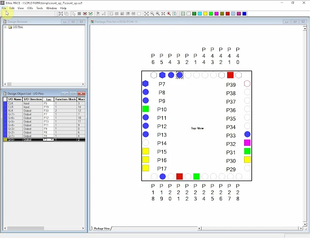
We need to assign inputs and output for this design using Xilinx PACE.
 |
| Pin Assignments |
After the pin assignments completed we click save and close this windows. The ISE will generate a user constraints file.
#PACE: Start of PACE I/O Pin Assignments
NET "BLK" LOC = "P33" ;
NET "CLK" LOC = "P5" ;
NET "CLR" LOC = "P19" ;
NET "Q<0>" LOC = "P3" ;
NET "Q<1>" LOC = "P4" ;
NET "Q<2>" LOC = "P8" ;
NET "Q<3>" LOC = "P9" ;
NET "Q<4>" LOC = "P11" ;
NET "Q<5>" LOC = "P13" ;
NET "Q<6>" LOC = "P12" ;
NET "Q<7>" LOC = "P7" ;
#PACE: Start of PACE Area Constraints
#PACE: Start of PACE Prohibit Constraints
#PACE: End of Constraints generated by PACE
 |
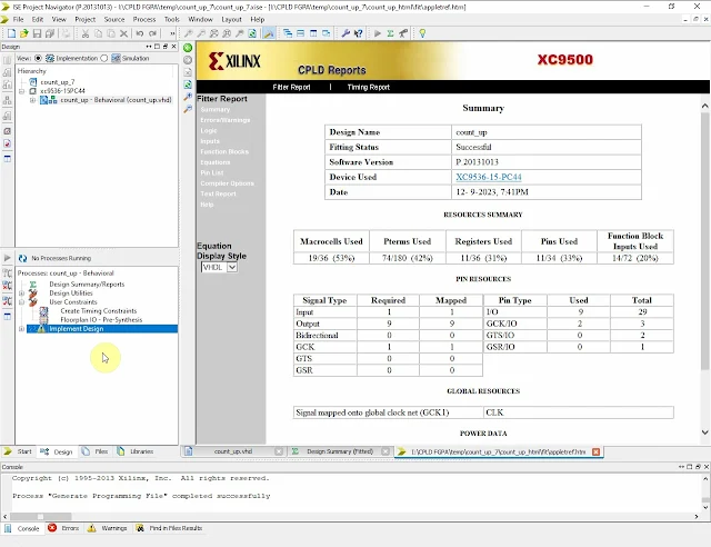
| CPLD Reports |
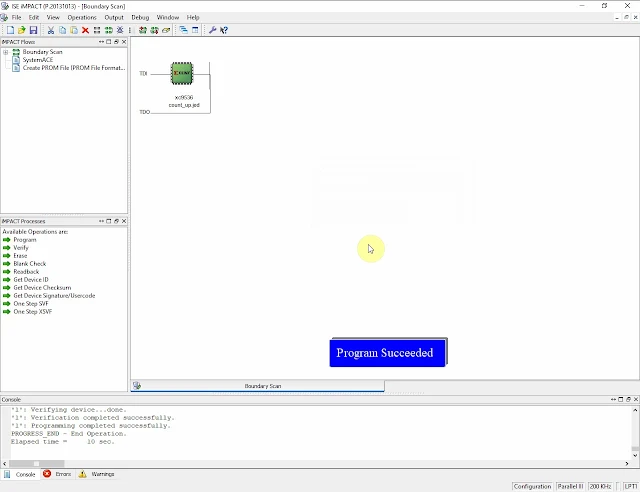
Device Programming
After the Pin Assignments is ready we have to re-run the Implement Design again to get a *.jed programming file. It will be used to upload to the XC9536 internal Flash memory.
 |
| Device Programming |
This parallel port JTAG header must be unplug after use because it has a detection pin on PC parallel port.
Click here to download its source file.
No comments:
Post a Comment