Overview
A serial in parallel out shift registers is very useful for I/O expanding. For instance, they can use it for driving multiple seven segments display, a dot matrix display, multiple output relays, etc. Standard serial-in-parallel-out shift registers ICs usage are the SN74HC595 and SN74HC164. They are very easy to find at very low cost. The controller uses only a few output pins to control these chips.
 |
| A 4-Digit Common Anode SN74HC595N Serial Display |
In this example, I designed an 8-bit serial-in-parallel-out shift registers using an XC9536 CPLD. All components are already placed on board. Its inputs outputs are listed below,
- Reset
- Clock
- Data
- Output
There's no output enable signal, or a 8th bit output for cascading. This circuit receive the least significant bit (LSB) first. So it shifts from left to right.
 |
| XC9536 Prototyping Board |
VHDL Code
Its VHDL code is quite simple. I added one 8-bit signal to process serial data reception. This design a sequential process.
Pin Assignments
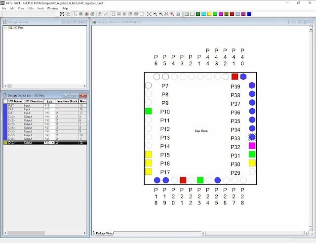
I use the Xilinx PACE Tool to set its I/O pins as follow.
 |
| Xilinx PACE |
After we save and close this windows, a user constraint file will be created.
Device Programming
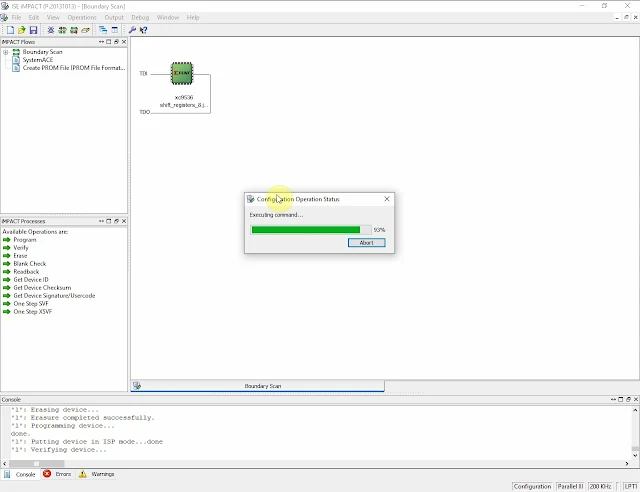
A parallel port JTAG cable is preferred since I write this code on a desktop computer that has an LPT-25 connector.
 |
| Device Programming Using Xilinx Parallel Cable III JTAG |
Click here to download its source file.
No comments:
Post a Comment