Digital I/O
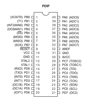
The ATMega16 AVR has up to four digital Input/Output ports. Those ports are bidirectional read/write port.
 |
| ATMega16 40-pin DIP pin diagram |
These four digital I/O ports are,
- Port A – PA
- Port B – PB
- Port C – PC
- Port D – PD
Each port is 8-bit wide. Beside the digital I/O function, these ports have other purposes,
- external interrupt
- counter inputs
- PWM outputs
- SPI/TWI communication
- USART communication
- Analog inputs, etc.
PORT Register And Direction Control
Output Direction
Each port is configurable as a digital input, or a digital output. The PORTx is an output register. To configure the any port as an output port, its corresponding data direction register, DDRx register must set.
As an instance, the programmer needs PA to output its digital data. The assignment in a C code must be set as follow,
DDRA=0xFF;   //PORTA is a fully output port
PORTA=0xAA;  //Output the hex value AA from PORTA
Let see another example, the lower nibble of PB is the output.
DDRB=0x0F;   //PORTB3.0 are the outputs
PORTB=0x02   //Set the output bit 1 of PORTB
Input Direction
A DDRx register must be cleared to configure the corresponding port as a digital input. PINx is its corresponding input buffer. Reading from the PINx register to get the logic state of the digital inputs.
For example, all bits of PA are the digital input.
DDRA=0x00;     //Configure PA as digital input
myState=PINA;  //Read the digital input logic state from PA
As in this instance, the lower nibble of PB is a digital input part.
DDRB=0xF0;         //PB3.0 are the digital input bits
myState=0x0F&PINB  //Read the digital input at the lower nibble
Digital Port Internal Weak Pull Up Resistors
For most of PIC microcontroller users, they usually think about the PORTB internal weak input pull up resistor. However, in the ATMega16 microcontroller every ports have their own internal weak pull up resistors. Each weak pull up resistor of one port is individually configurable.
This feature is commonly used in the input direction. To turn on the internal weak pull up resistors,
- Set the data direction to the input
- Write a preferred value to the PORTx register
For example, a lower nibble of PD is a digital input. The programmer turn on the internal weak pull up resistor of this lower nibble.
DDRD=0xF0;   //PIND3.0 are the digital inputs
PORTD=0x0F;  //Turn on the weak pull up resistors of the PINC3.0
Atmel Studio 7 C Programming
Overview
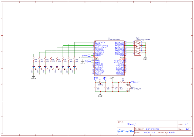
Within this introductory example, I select port A as a digital input port. PB is configured as a digital output port. The main program loop reads the digital data from PINA, while port b output this digital data. We don’t need to add any external resistors to the digital input pins since the programmer just need to write 0xFF to PORTA.
We need to know about port A register associations.
 |
| Port A Data Register – PORTA |
 |
| Port A Data Direction Register – DDRA |
 |
| Port A Inputs Pin Address – PINA |
Finally, the registers associate to port B list below.
 |
| Port B Data Register – PORTB |
 |
| Port B Data Direction Register – DDRB |
Schematic Diagram
I draw the schematic diagram of this example using a free EDA software. It follow the hardware configuration on my development board I designed.
 |
| Schematic Diagram |
The supply voltage is +5 V DC to clock the CPU to its maximum 16 MHz frequency.
Atmel Studio 7 C Code
I migrated my code writing from the AVR Studio to Atmel Studio for a few years now. I started with the earlier version Atmel Studio 6 in 2017.
Click here to download the zip file of this example.
 |
| A program testing on the development board |

No comments:
Post a Comment