About Proteus
Proteus VSM is an EDA software owns by Labcenter Electronics from the UK. It offers the the simulation of the analog, digital circuit using SPICE. Simulating the microcontroller/microprocessor is also a good option. It’s a paid software. However I share the license of this software with the company I’m working.
Beside the simulation in this software, the designer could create a circuit board design of the corresponding project. The circuit board design using Proteus takes a shorter time than other EDA software as I have been work with it for many years now. It has a lot of symbols and footprint library. The schematic and PCB design process is simple because we don’t any complex step.
Why Gerber ?
Gerber file format is a standard uses by the PCB industry. It contains the graphic of the design PCB such as copper layer, silk screen layer, drill size, etc.
The designer have to make this file to before the design is sent to the PCB manufacturer. However for a DIY PCB making, especially for the hobbyist, it’s not always need this file format. A single side PCB that will be fabricate by hand with a few amounts could be done by a simple toner transfer method, a silk screen process or a DIY dry film process.
Getting The Design Ready
I don’t show any detail of the circuit board design here because the article will take so long. Designing the circuit board process must be shown in a video tutorial.
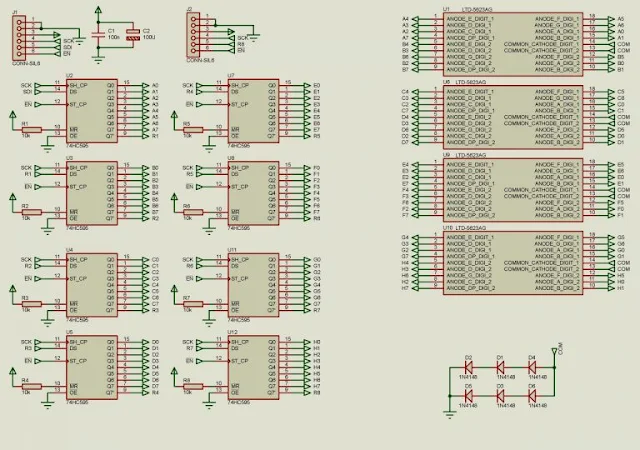 |
| A Sample Schematic |
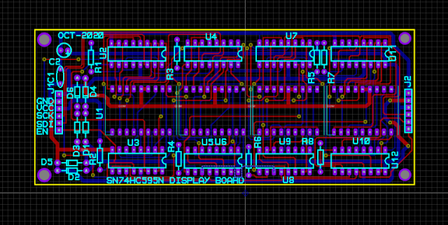 |
| A Sample PCB |
For most of the PCB design, the designer must very the design individually. It’s assumed that the project really work before starting the PCB design. As I have experienced the common mistake of the design is setting a right drill hole of the specific on-board components.
Using a service from the PCB manufacturer, the fabricated PCB must be at least a double-sided PCB to ease the soldering/assembling of the project. The drill hole always plated while it’s in manufacturing. Selecting a larger drill hole of a specific component doesn’t matter. However selecting a smaller drill hole of the component, the inserting doesn’t fit. The drill plated holes could be work again manually. But drilling the plated hole could make the disconnection of the circuit inter-connect. It makes trouble to the working project.
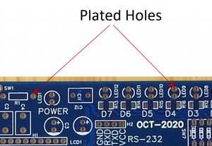 |
| Plated holes of the fabricated PCB from manufacturer |
Creating Gerber File
Each layer of the PCB has its own Gerber file. The overall design consists of many Gerber file. The file format is in text file that will be interpreted by software. For most common, the Gerber files are zipped in a single zip file.
In Proteus PCB Layout, go to Output -> Generate Gerber/Excellon Files.
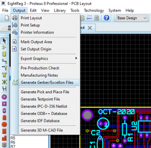 |
| Generate Gerber Files |
The pre-production checking prompt will display. We can ignore it by clicking NO.
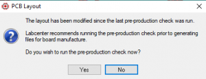 |
| Running or ignoring the pre-production check. |
All layers in the design are ticked in the CAD/CAM Output. The user can select or deselect any layer. The Gerber files are zipped in one zip file.
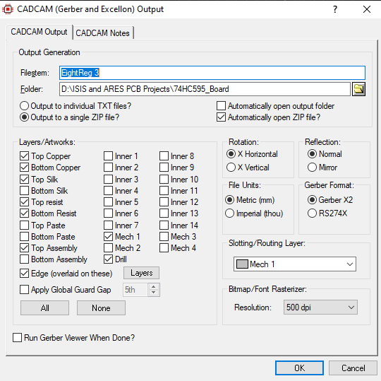 |
| CAD/CAM Output |
Click OK to create.
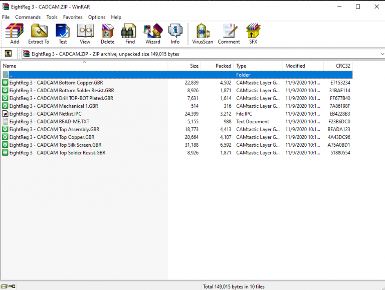 |
| A created zip file of the Gerber files |
This file will be uploaded to PCB manufacture website for ordering.
Putting An Order Of The Design
There are many PCB manufactures that we can put an order online. I have been a customer of PCBWay. It takes only a few days to get the PCB to my workplace after I put the order, and make payment.
On the manufacturer quick online order page, upload your design and get quote.
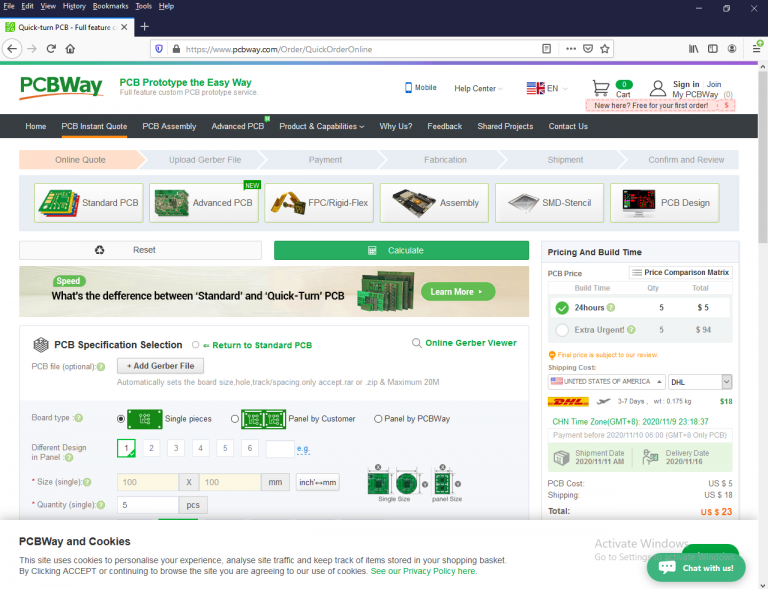 |
| Quick Order Page Of PCBWay |
Click on Add Gerber File to select and upload the zipped Gerber files that has just created by Proteus.
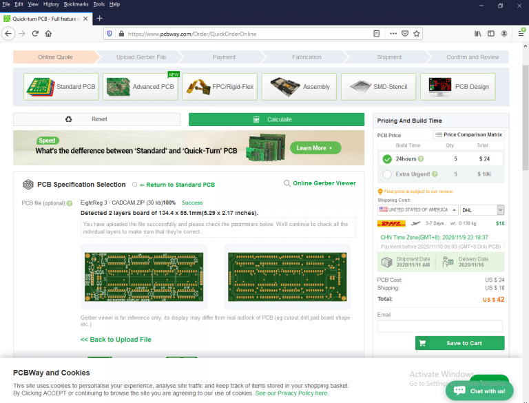 |
| An uploaded Gerber format |
The page will automatically determine the dimension and the number of layers. What the user select are,
- the thickness of the board
- color of solder mask and silk screen
- copper thickness
- pad plating, etc.
I don’t list them all here because it’s the choice of customer. As I have ordered from this manufacturer, the processing time is less than 24 hours to complete. The delivery time takes only one day to arrive at my warehouse.

No comments:
Post a Comment