Introduction
I have been an electronics hobbyist/designer for many years now, designing and prototyping some electronic projects for my own leisure and also selling them to the markets. In an electronic projects, the Printed Circuit Board (PCB) is an important part that keep all components together, getting them connected on the traces by the term of soldering.
 |
| Some Fully tested PCB projects I made by myself. Some’s are made with the toner transfer method, while the other’s are made with the UV dry-film method. |
A DIY Toner Transfer Method
Some uncomplicated PCB projects only require a single sided PCB that could be easily made by hand, using a toner transfer method. As an example, all the PCB project as shown in the picture above are single sided with the aid of wire jumpers. The PCB tracks protection are the laser printer’s toner that transfer from the printed glossy paper.
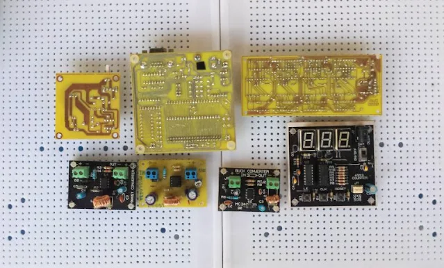 |
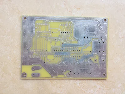
| These completed PCB projects made using the toner transfer method. It works well. There are some corrosion on the PCB track due to low quality of the printing toner. |
 |
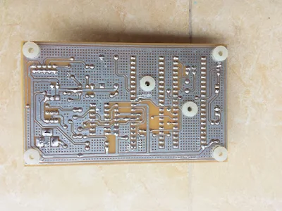
| This is an Arduino Shield pre-etching. The circuit pattern on the copper is laser printer toner. It protect the the coating area from being etched. |
A hot plate lamination or an electric iron transfer its heat with pressure to force the toner stick on the cleaned copper area of the copper clad board. The PCB etchant is typically a low cost Ferric Chloride acid solution with a 1:4 mixing ratio. This type of acid solution could be keep for a few years.
After the PCB etching is ready the PCB must be cleaned, cut and drilled. A solder mask must applied to the copper side to protect the PCB from corrosion. However without a solder mask ink, we can use a tin-lead solder to protect the copper circuit pattern. The soldering paste must be applied to the circuit pattern before or while the tin-lead solder is applying with hot electric soldering iron.
Applying a tin-lead over the copper circuit pattern is not hard. It takes only a half of hour, depending on the size of the PCB and quality of the materials in use.A DIY PCB made with the toner transfer method is effective for only a single sided PCB. However the circuit design with a double side PCB requires a higher technical method – a dry film method. This method requires a UV dry film with some photo chemical materials and a UV light bulb to create the circuit pattern. For an electronic hobbyist that use his/her own equipments, it take a very long time and more skills to make it done. This method has been using by the PCB manufacturing industry. Currently it’s still to develop by many companies. I will not list the details of this method here due to some constraints.
Using An Affordable PCB Service
For a more complex design, it requires more than one copper side of the PCB. In this case a double sided or a multi-layers PCB is needed. A complex design is regardless of the hobbyist projects. For the hobbyist it’s very hard, time consuming and costly to make this job done. For convenience, hobbyist/developer must use a PCB fabrication service available world wide. Currently this service is very competitive. The provider offer an affordable price of the printed circuit with many options.
 |
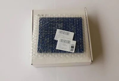
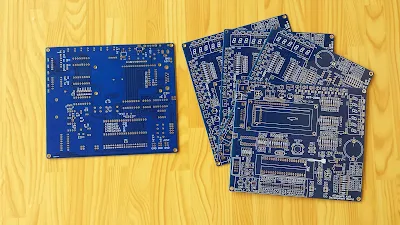
| A pack of PCB I ordered from PCBWay It’s an ATMega16 Development board that I will use it for the tutorials on this site. The PCB is double sided with a blue solder mask and white components legend. |
I have been a customer of PCBWay for a period of time now. The cost of the printed circuit from this company is reasonable. The processing time is very fast. As an example of the PCB shown above the PCB manufacturing takes less than 24 hours through many technological steps to complete. The delivery time take only two days after the PCB is shipped out.
 |
| The manufacturing process of this order takes during one day. |
So it spends only a few day after I put the order and send the payment to get the printed circuit boards to my warehouse.
 |
| A completed PCB assembling of an ATMega16 microcontroller development. It’s a double-sided PCB. I selected a 1 mm thickness of the panel. The PCB manufacturer offers up to 14 layers. |
Finally we can spend the time doing other task rather than trying to fabricate the PCB by ourselves. The quality of the boards from this service is great like the commercial products on the market.
"Wow, I came to learn about machines, and your information is absolutely amazing! For more insights and if your are looking for the Fabrication services.com!
ReplyDelete! We specialize in reliable solutions to meet all your welding needs. Keep up the great work!"