Introduction
Analog-to-Digital Converter (ADC) module of a microcontroller converter analog input voltage to digital value representation that microcontroller process with. There are many different types of ADC module inside microcontroller.
ADC module has some parameters:
- Resolution : Define the amount of digital number of analog to digital conversion. It could be 8-bit, 10-bit, 12-bit, etc. Larger resolution gives the conversion result more accurate.
- Voltage reference: It also effect Resolution. Lower voltage reference of ADC makes an accurate conversion result. It could be 2.5V, 3.3V, or 5V.
- Clock : It could be driven from microcontroller clock source, or its own internal clock.
- Number of Analog Input Channel : It refers to the amount of input pins of ADC. It usually multiplexed with other digital I/O pins.
The figure below is ADC block diagram of PIC16F887.
 |
| Block diagram of PIC16F887 ADC Module |
Programming for ADC
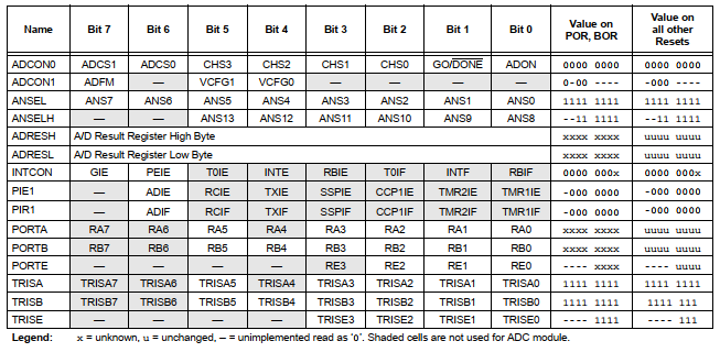
ADC module inside PIC16F887 has some registers for programmer to work with. Programmer need to configure,
- ADC clock
- Analog channel inputs
- Result arrangement
- Channel selection
- Start of conversion
- Testing the result and reading the result
- Interrupt control (optional)
These registers are,
 |
| Registers relate to ADC of PIC16F887 |
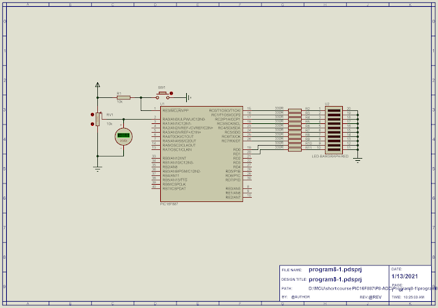
Now let start a simple example of using ADC module. This program read analog input on RA0/AN0. Conversion result will display on Port C and Port D.
 |
| Schematic Diagram |
MikroC source code:
Click here to download zip file of this working example.